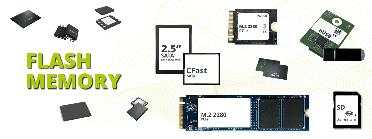
Flash Memory
Flash memory is a non-volatile memory that can be electrically programmed, erased, and reprogrammed. There are two main flash memory types, NAND Flash and NOR Flash, that are named after their differing gates.
It was invented by Toshiba in 1980 when Fujio Masuoka proposed a new type of floating-gate memory that allowed entire sections of memory to be erased by applying voltage to a group of cells with a single wire. The name flash was suggested by a colleague because the erasure process reminded him of a camera flash. Fujio Masuoka and his team refined the memory and presented the invention of NOR flash in 1984 and the invention of NAND flash three years later, in 1987.
NOR flash is known for its direct random-access capabilities, making it ideal for direct code execution.
NAND has to be read block-wise, but NAND cells are 60% smaller than NOR cells, thus allowing greater storage density and lower cost per bit. This makes NAND ideal as second-level storage such as memory cards.
NOR Flash
There are two types of NOR flash memory: Parallel NOR Flash and Serial NOR Flash with the main difference in the way the memory is accessed. Serial NOR Flashes are accessed via SPI, therefore having a low pin count whereas parallel NOR flashes are accessed via the usual data/address bus.
Serial NOR Flash
Serial NOR is a very common technology, as its SPI-interface is widely used in communication equipment.
There are several different SPI NOR Flash options available: single, double, quad, and even octal SPI NOR Flash. The multiples of SPI refer to the number of SPI channels that a device offers. Quad SPIs are suitable for direct code execution, provided the CPU attached offers this option.
NAND Flash
NAND flash memory, also known as raw NAND, consists of only the memory chip. Because NAND has a limited number of write times, an external controller is needed to make sure that data is not always written to a fixed location but spread evenly across all cells. Its advantage is the low cost per bit and its capacity. There are several types of raw NAND flash memory.
Serial / SPI NAND
Serial or SPI NAND organizes the memory cells of a NAND memory into a row of serial banks. It is a low-cost memory with a small form factor that makes it ideal for code handling in space-constrained embedded applications like smartwatches, medical devices or various automotive environments.
Parallel NAND
Parallel NAND Flash is a type of NAND Flash memory that is organized into multiple parallel banks, rather than a single serial bank. This allows for much higher data throughput than other memory devices, making it ideal for applications that require high data bandwidth. This memory utilizes the 8-bit multiplexed bus to provide much faster data transferring, addressing, and processing.
SLC, MLC, TLC, QLC Flash
- SLC, or single-level cells, store one bit per cell. SLC has the highest endurance, fastest write speed and lowest power consumption. However, it is also the most expensive type of NAND flash storage as it has about 100,000 write cycles per cell before deteriorating.
- MLC, or multi-level cells, stores two bits per cell thus double the amount of data in the same sized device. This reduces the costs per bit. However, MLC only supports about 10,000 write cycles. So it’s a good memory choice for high-density but low-cycle applications.
- TLC, is able to store three bits per cell. The higher capacity comes at a trade-off: it can only support 4,000 write cycles per cell before deteriorating.
- QLC, or quad-level cells, store four bits per cell. QLCs have even less endurance and are generally less expensive.
3D NAND
2D or planar NAND has only one layer of memory cells, whereas 3D NAND stacks cells on top of one another. Samsung refers to 3D NAND as Vertical NAND or V-NAND.
Contact us if you are looking for a specific product
