

Dynamic Random-Access Memory (DRAM) has been central to advances in computing performance for decades. Each successive generation has achieved significant gains in speed, density, and energy efficiency to meet the demands of data-centric applications. As DDR5 adoption matures, the industry is preparing for DDR6, the sixth generation of Double Data Rate Synchronous DRAM. Expected to enter production in late 2025 or early 2026, DDR6 promises to redefine performance benchmarks across artificial intelligence (AI), cloud infrastructure, high-performance gaming, and enterprise workloads.
This paper synthesizes available draft specifications, as well as vendor and JEDEC working group insights, to provide a comprehensive overview of DDR6 development timelines, architectural innovations, comparative performance metrics, and market adoption trends.
Since the commercial debut of DDR5 in 2021—aligning with AMD Ryzen 7000 and Intel Alder Lake architectures—memory technology has evolved to support exponential increases in bandwidth and efficiency. DDR5 achieved substantial improvements over DDR4, including dual sub-channel design and increased transfer rates. However, the rising computational demands of AI model training, real-time analytics, and immersive gaming have underscored the need for a new generation of memory.
DDR6 is being standardized by the JEDEC JC-42.3 subcommittee, with a projected release of Specification 1.0 in 2025. Initial prototypes from leading DRAM manufacturers indicate transformative capabilities in throughput, power optimization, and memory architecture.
The progression of DDR standards follows a consistent cadence of approximately five-year intervals, with each generation doubling the maximum data transfer rate. The timeline for DDR6 development is as follows:

| Standard | Max JEDEC Data Rate (MT/s) | Year Introduced |
|---|---|---|
| DDR | 400 | ~2000 |
| DDR2 | 800 | ~2003 |
| DDR3 | 1,866 | ~2007 |
| DDR4 | 3,200 | ~2014 |
| DDR5 | 6,400 | ~2020 |
| DDR6 | ≥12,800 (Projected) | ~2025–2026 |
This structured standardization process ensures that DDR6 will be interoperable across CPU, SoC, and DIMM suppliers, accelerating time to market once finalized.
DDR6 is expected to double maximum data transfer rates relative to DDR5. Projections indicate:
These speeds will enable memory bandwidths exceeding 134 GB/s per DIMM, supporting increasingly data-intensive applications.
DDR6 introduces multiple architectural innovations designed to improve throughput and efficiency:
DDR6 is projected to achieve significant power reductions:
These advances will be essential for sustainable data centers, edge computing, and mobile devices.
Table 2. Historical and Technical Comparison of DDR Memory Standards
| Parameter | DDR | DDR2 | DDR3 | DDR4 | DDR5 | DDR6 (Projected) |
|---|---|---|---|---|---|---|
| JEDEC Max Data Rate (MT/s) | 400 | 800 | 1,866 | 3,200 | 6,400 | ≥12,800 |
| Overclocked Potential (MT/s) | ~550 | ~1,066 | ~2,133 | ~4,000 | ~8,400 | ≥15,000–17,000 |
| Typical Voltage | 2.5 V | 1.8 V | 1.5 V (1.35 V LP) | 1.2 V | 1.1 V | <1.1 V |
| Burst Length | 2, 4, 8 | 4, 8 | 8 | 8 | 16 | 16 |
| Prefetch Buffer | 2n | 4n | 8n | 8n | 16n | ≥16n |
| Channels per DIMM | 1 | 1 | 1 | 1 | 2 | 4 |
| Sub-channel Width | 64 bits | 64 bits | 64 bits | 64 bits | 32 bits | 16 bits |
| DIMM Max Bandwidth | ~3.2 GB/s | ~6.4 GB/s | ~14.9 GB/s | ~25.6 GB/s | ~51.2 GB/s | ≥134 GB/s |
| CAS Latency (Cycles) | 2–3 | 3–6 | 5–11 | 10–19 | 20–40 | TBD (Expected ≥40) |
| Refresh Modes | Auto/Manual | Auto/Manual | Auto/Manual | Auto/Manual | Same as DDR4 | Adaptive Refresh |
| Power Saving Features | Basic | Partial Array SR | Partial Array SR | DBI, CA Parity | DVFS, On-die ECC | DVFS, Sideband Telemetry |
| Signal Integrity Enhancements | Basic termination | ODT | Fly-by topology | DFE, ODT | DFE, ODT | DFE, CTB, Sideband |
| Error Correction | No (Optional ECC) | No (Optional ECC) | Optional ECC | Optional ECC | On-die ECC | Enhanced On-die ECC |
| Typical Power Consumption | High | Moderate | Moderate | Lower | Lower | Significantly Lower |
| Target Markets (Initial) | Desktop | Desktop, Server | Desktop, Server | Server, Desktop | Server, Desktop | HPC, AI, Cloud, Enterprise |
DDR6’s performance and efficiency improvements make it especially well-suited for:
The transition to DDR6 is anticipated to follow the pattern observed in prior DRAM migrations, characterized by an initial phase of limited deployment in specialized domains before mainstream adoption.
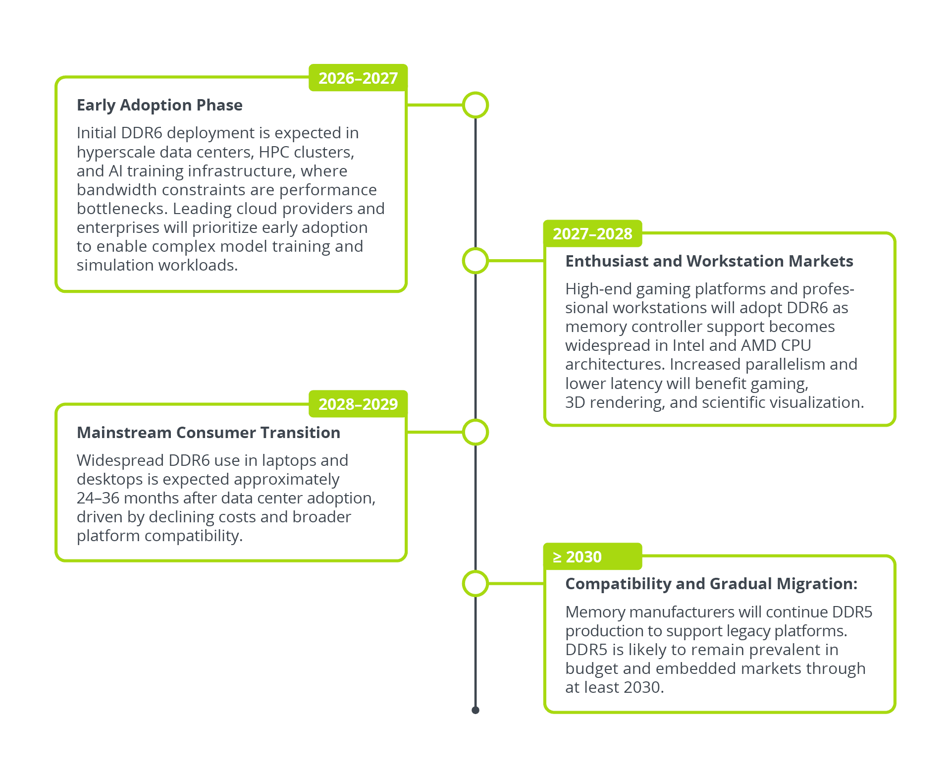
Overall, DDR6 adoption is expected to proceed more rapidly than DDR5 but may still require 5–6 years to reach majority penetration.
DDR6 represents the next transformative advance in DRAM technology, combining unprecedented bandwidth, improved power efficiency, and architectural flexibility. While the specification is pending JEDEC ratification, consensus indicates DDR6 will soon become foundational to high-performance computing ecosystems across AI, cloud, gaming, and enterprise workloads.
The coming years will define the trajectory of memory innovation—and DDR6 is positioned to lead that evolution.
Contact our technical sales team to request engineering samples, integration support, or design-in consultations.